
Edit: It is! I got the WiFi replaced and functional.
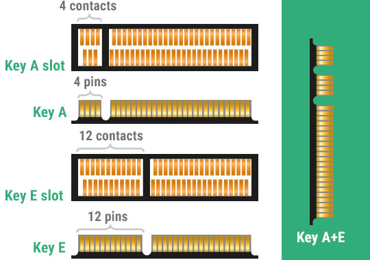
I need a confirmation that this is an accurate diagram, I have a A+E-key WiFi adapter, and I need to use it to replace a E-key WiFi adapter. I cannot find much information about compatibility, and need some confirmation before I stick my adapter in a type-e slot.
Did you not notice the staggered pinout on the diagram? That looks like it’s literally designed to be a short circuit no matter what the manual says.
I’ve literally dealt with staggered pin short circuits twice in my life, one from equipment damage, and another from piss poor engineering.
Either way it’ll totally fry the power supply, if not more…
I thought the staggered contacts engage with similarly staggered pins on the other side of the card?? 🤔
You are right. The user you are replying to has no idea what they write about, as they confessed in another comment.
I’m not hands on familiar with these standards, so I’m not entirely sure. But when I see a diagram showing 4 pins on one side and 3 pins on the other, but the card going into it only shows one side, then it raises immediate red flags of incomplete information.
No worries, my card has 4 on one side and 3 on the other, so I don’t believe that will be an issue. I thought that you were more concerned about the slight difference in the pin’s location from top to bottom of the slot diagram.
Cool cool. I was worried that it might be a piss poor diagram made by a 10 year old just learning Photoshop or something.
When it comes to electronic diagrams, I’m used to seeing complete pinouts that label every single pin, like ground, power, data and clock signals and whatnot.
Seeing such an incomplete diagram like this one just scares me though.